- 您现在的位置:买卖IC网 > Sheet目录539 > ZXMC10A816N8TC (Diodes Inc)MOSFET DUAL COMPL 100V 8-SOIC
ZXMC10A816N8
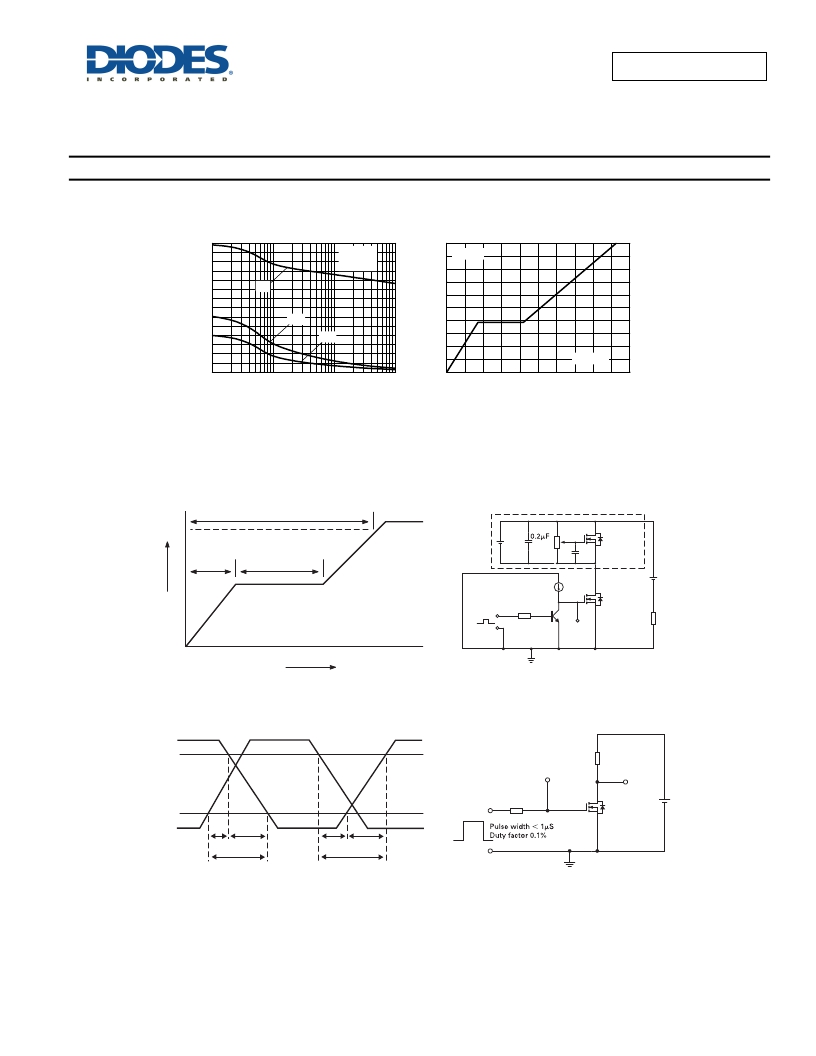
Typical Characteristics Q1 N-Channel (cont.)
700
10
600
500
400
300
200
100
C ISS
C OSS
C RSS
V GS = 0V
f = 1MHz
8
6
4
2
I D = 1.6A
V DS = 50V
0
0.1
1
10
100
0
0
2
4
6
8
10
V DS - Drain - Source Voltage (V)
Capacitance v Drain-Source Voltage
Q - Charge (nC)
Gate-Source Voltage v Gate Charge
Test Circuits
Current
regulator
Q G
12V
50k
Same as
D.U.T
V G
Q GS
Q GD
Charge
I G
V GS
D.U.T
V DS
I D
V DS
Basic gate charge waveform
Gate charge test circuit
90%
10%
V GS
R G
V GS
R D
V DS
V DD
t d(on)
t (on)
t r
t d(off)
t (on)
t r
Switching time waveforms
Switching time test circuit
ZXMC10A816N8
Document number: DS33497 Rev. 2 - 2
6 of 11
www.diodes.com
March 2013
? Diodes Incorporated
发布紧急采购,3分钟左右您将得到回复。
相关PDF资料
ZXMC3A16DN8TA
MOSFET N+P 30V 5.4A 8SOIC
ZXMC3A17DN8TC
MOSFET N/P-CHAN DUAL 30V 8SOIC
ZXMC3A18DN8TA
MOSFET N-CH/P-CH 30V 8-SOIC
ZXMC3AM832TA
MOSFET N+P 30V 2.7A 8MLP 3 X 2
ZXMC3AMCTA
MOSFET N+P 30V 2.9A/2.1A DFN
ZXMC4559DN8TA
MOSFET N/P-CHAN DUAL 60V 8SOIC
ZXMC4A16DN8TC
MOSFET N/P-CHAN DUAL 40V 8SOIC
ZXMD63C03XTC
MOSFET N/P-CHAN DUAL 30V 8MSOP
相关代理商/技术参数
ZXMC3A16DN8
制造商:DIODES 制造商全称:Diodes Incorporated 功能描述:COMPLEMENTARY 30V ENHANCEMENT MODE MOSFET
ZXMC3A16DN8_05
制造商:ZETEX 制造商全称:ZETEX 功能描述:COMPLEMENTARY 30V ENHANCEMENT MODE MOSFET
ZXMC3A16DN8TA
功能描述:MOSFET N and P Channel RoHS:否 制造商:STMicroelectronics 晶体管极性:N-Channel 汲极/源极击穿电压:650 V 闸/源击穿电压:25 V 漏极连续电流:130 A 电阻汲极/源极 RDS(导通):0.014 Ohms 配置:Single 最大工作温度: 安装风格:Through Hole 封装 / 箱体:Max247 封装:Tube
ZXMC3A16DN8TC
功能描述:MOSFET Cmp 30V NP Ch UMOS RoHS:否 制造商:STMicroelectronics 晶体管极性:N-Channel 汲极/源极击穿电压:650 V 闸/源击穿电压:25 V 漏极连续电流:130 A 电阻汲极/源极 RDS(导通):0.014 Ohms 配置:Single 最大工作温度: 安装风格:Through Hole 封装 / 箱体:Max247 封装:Tube
ZXMC3A17DN8
功能描述:MOSFET N and P Channel RoHS:否 制造商:STMicroelectronics 晶体管极性:N-Channel 汲极/源极击穿电压:650 V 闸/源击穿电压:25 V 漏极连续电流:130 A 电阻汲极/源极 RDS(导通):0.014 Ohms 配置:Single 最大工作温度: 安装风格:Through Hole 封装 / 箱体:Max247 封装:Tube
ZXMC3A17DN8_05
制造商:ZETEX 制造商全称:ZETEX 功能描述:COMPLEMENTARY 30V ENHANCEMENT MODE MOSFET
ZXMC3A17DN8TA
功能描述:MOSFET 30V Enhancement Mode RoHS:否 制造商:STMicroelectronics 晶体管极性:N-Channel 汲极/源极击穿电压:650 V 闸/源击穿电压:25 V 漏极连续电流:130 A 电阻汲极/源极 RDS(导通):0.014 Ohms 配置:Single 最大工作温度: 安装风格:Through Hole 封装 / 箱体:Max247 封装:Tube
ZXMC3A17DN8TC
功能描述:MOSFET 30V Enhancement Mode RoHS:否 制造商:STMicroelectronics 晶体管极性:N-Channel 汲极/源极击穿电压:650 V 闸/源击穿电压:25 V 漏极连续电流:130 A 电阻汲极/源极 RDS(导通):0.014 Ohms 配置:Single 最大工作温度: 安装风格:Through Hole 封装 / 箱体:Max247 封装:Tube